 TFStudio
Synthesizing a Four-Line Multipassband Filter with Needle
Carve a four-line transmission filter out of a single thick TiO2 layer using Needle, Design Cleaner, and a constrained SQP refinement.
The previous optimization tutorial refined a four-layer AR coating. Four thicknesses moved, and the structure never changed. That is all refinement can do. If a design needs more layers than it has, or needs them in a different order, no amount of thickness refinement will get there.
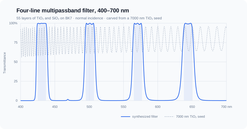
This tutorial does the opposite kind of work. The target is a four-line multipassband transmission filter: four narrow bands that must pass, everything between them blocked. The starting point is a single 2500 nm slab of TiO₂, which resembles nothing about the answer. Needle synthesis will carve it into a 55-layer filter with four lines above 97.5% average transmittance and stopbands below 2.5%, in about eight minutes of work.
The same exercise ships inside TFStudio as the Multipassband filter: Needle + Cleaner tutorial (Help → Tutorials). This article follows that task but pushes it further than the in-app version does, with a higher layer budget, a manufacturing thickness constraint, and a final refinement pass. The in-app tutorial stays deliberately short.
The design conditions
- Incident medium: Air
- Substrate: BK7 (Schott)
- Coated surface: Front
- Evaluation: Ignore other side
- Angle of incidence: 0°
- Polarization: Average
- Reference wavelength: 550 nm
- Materials: TiO₂ and SiO₂ only
The in-app tutorial registers a dedicated two-material catalog, Multipassband (TiO2/SiO2), and uses it for both the seed layer and the Needle candidate pool. A two-material pool suits this exercise, where structure rather than material variety does the work.
| Catalog entry | at 400 nm | at 550 nm | at 700 nm |
|---|---|---|---|
TiO2 |
2.7734 | 2.5166 | 2.4468 |
SiO2 |
1.4701 | 1.4599 | 1.4553 |
BK7 (Schott) |
1.5308 | 1.5185 | 1.5131 |
Both coating materials are treated as non-absorbing across 400–700 nm, so the filter's stopbands work by reflection rather than absorption.
Why the starting design is one thick layer
Needle synthesis inserts an infinitesimally thin layer of a candidate material at the position where it most improves the merit function, then refines (Sullivan & Dobrowolski 1996; Tikhonravov et al. 1996). The insertion has no thickness of its own. It splits an existing layer in two and puts a new interface between the halves.
That has a direct practical consequence: needle can add interfaces, but not optical thickness. A filter of this kind needs several micrometres of material to build four narrow lines with steep edges. If synthesis starts from a thin stack, needle has nothing to subdivide and stalls at a shallow design. Starting from a thick slab gives it bulk to work with, and the refinement between insertions redistributes that bulk.
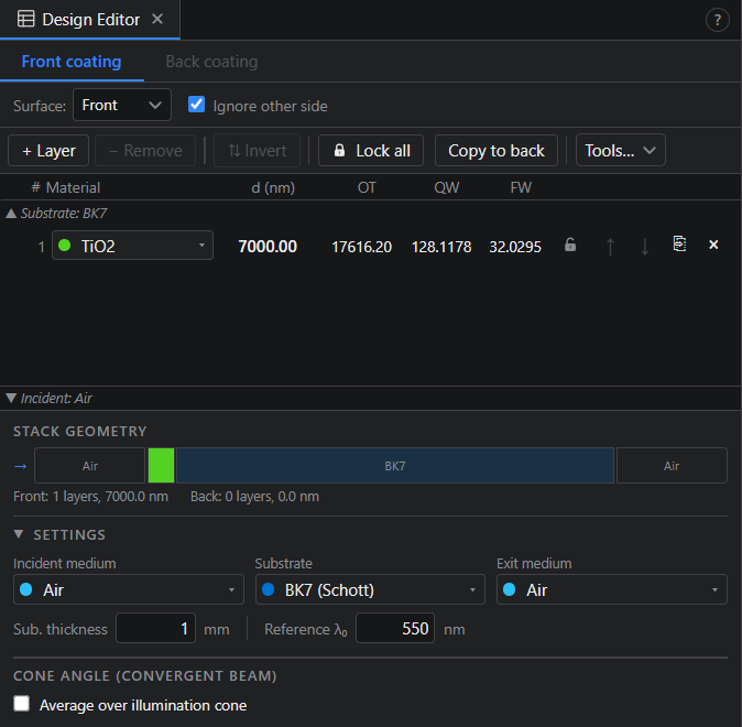
So the starting design is a single layer:
| Design Editor layer | Material | Thickness |
|---|---|---|
| 1 | TiO2 |
2500 nm |
Define the merit function
The target is four passbands and the five stopbands between and around them, all specified as band averages of transmittance. Open the Merit Function Editor and enter nine TAV operands, all at 0° with average polarization and weight 1:
| Operand | Band | Target | Step |
|---|---|---|---|
TAV |
425–437 nm | 0 | |
TAV |
495–507 nm | 0 | |
TAV |
565–577 nm | 0 | |
TAV |
638–650 nm | 0 | |
TAV |
400–420 nm | -0.25 | |
TAV |
442–490 nm | -0.25 | |
TAV |
512–560 nm | -0.25 | |
TAV |
582–633 nm | -0.25 | |
TAV |
655–700 nm | -0.25 |
The Step column says how finely a band is sampled. 0 leaves it to the app, which spaces the samples by the design's interference fringes. A negative number is a step in nanometres, so the stopbands are sampled every 0.25 nm. A stack this thick has resonances narrower than its fringes, and in a stopband a resonance is a spike of transmission that falls between the samples, where the optimizer never sees it. The finer step lets it see more of them.
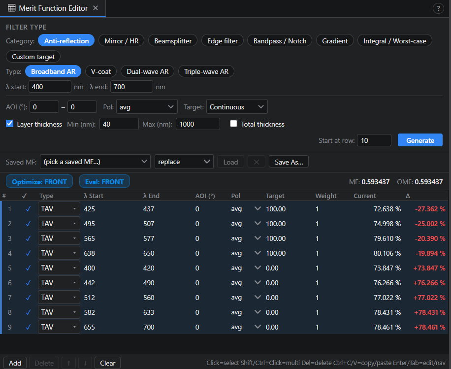
TAV is the average of transmittance over its band, so each operand contributes one number, and the merit function is the root-mean-square of the nine deviations from target:
Note the 5 nm guard between each passband and its neighbouring stopband. Nothing is specified between 437 and 442 nm, for example. Those gaps are where the filter edges are allowed to fall. Specifying a band edge as a step from to at a single wavelength asks for something no finite stack can deliver, and the optimizer will spend layers fighting it.
Leave thickness constraints out for now. Needle ignores MNT and MXT during synthesis anyway, and a manufacturing floor imposed this early only holds the search back.
The bare seed, for reference
Before running anything, look at Optical Evaluation. The 2500 nm slab is a thick etalon: dense interference fringes swinging between 55.5% and 95.8% transmittance across 400–700 nm, with no passband structure at all. Its merit function is 0.581064.
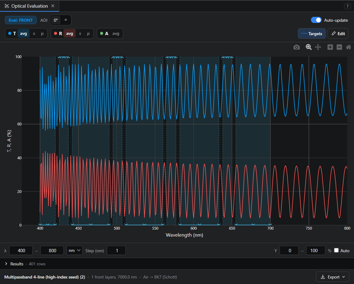
That number is the baseline for everything below.
Step 1. Needle
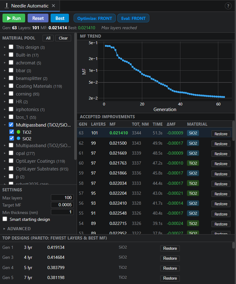
Open Needle Automatic and set:
- Candidate materials: TiO₂ and SiO₂ (the
Multipassband (TiO2/SiO2)catalog only) - Inner refiner: Conjugate Gradient
- Refine iterations: 30
- Max layers: 100
Press Run and watch two things: the layer count climbing as insertions are accepted, and the merit function dropping after each refinement. The scan plot shows the P-function against position, and its deepest dip is where the next needle goes.
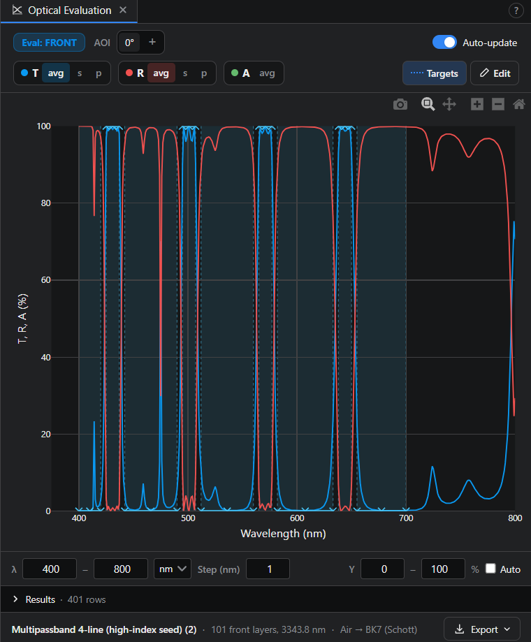
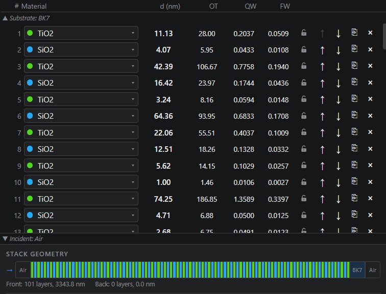
After about four and a half minutes it reached 101 layers and stopped. The merit function is down from 0.581064 to 0.024512, and the stack is 2801.73 nm thick, a little more than the seed: much of the slab is now SiO₂, which takes more nanometres for the same optical thickness. Much of what it built is too thin to deposit: the thinnest layer is 1.00 nm, and 47 of the 101 layers are under 5 nm.
Step 2. Design Cleaner
A stack straight out of needle contains layers that earn nothing: a few nanometres thick, sometimes sandwiched between two layers of the same material because an insertion was later refined down to nothing.
Open Design Cleaner, which removes layers below a thickness threshold, merges same-material neighbours, and re-refines to recover the merit the removals cost.
- Minimum thickness: 5 nm
- Merge adjacent: on
- Re-optimize after: on
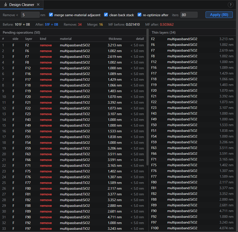
The operations preview lists every removal and merge with the merit function before and after, so the cost of the cleanup is visible before committing to it.
It lists 56 operations here, 47 removals and 9 merges, and the stack drops from 101 layers to 45. Removing a thin layer leaves its two neighbours touching, and when they are the same material the next pass merges them. Here the thin layers mostly sit side by side, so many removals leave two different materials touching and need no merge. Together the layers that go are about 90 nm of material, which is the point: they were carrying almost no optical thickness.
They were carrying some merit, though. Straight after the cleanup the merit function is more than twenty times worse than where needle left it, as the window's MF after shows. Re-optimize wins it back: it refines the cleaned stack with the refiner in the list beside it, Sequential QP here, and ends at MF 0.017188, below where needle stopped, with the stack grown to 3093.34 nm.
Step 3. Add a thickness floor and refine with SQP
The design is now structurally right but not yet manufacturable, since synthesis leaves layers thin enough that a deposition run could not hold them to tolerance. Deleting those layers would change the spectrum. Give the refiner a constraint instead and let it redistribute.
Back in the Merit Function Editor, add one operand:
| Operand | Layers | Target |
|---|---|---|
MNT |
all | 30 nm minimum |
Nine of the 45 layers are below 30 nm at this point, so the merit function jumps to 8.333351 the moment the operand goes in. That number is the constraint violation, not the optics: the optical part is still 0.017188. A hard constraint dominates the merit function until it is satisfied, which is exactly how it should behave.
Then open Refinement and run Sequential QP. SQP suits the problem now that it genuinely has constraints, because it handles the 30 nm bounds directly instead of penalizing violations after the fact. See Optimization Methods for how the methods differ.
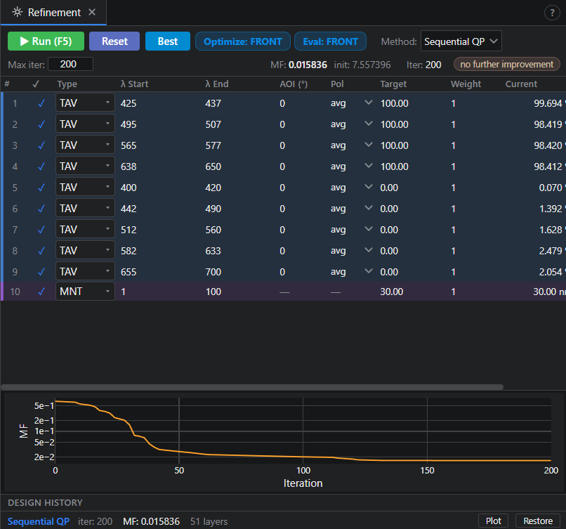
SQP satisfies every bound, and the floor has a price: it lands at MF 0.030352, above the 0.024512 needle reached with layers a nanometre thick, because 30 nm is thicker than some layers the optics wanted. Fourteen layers sit exactly at 30.00 nm, which is the signature of an active constraint: the optimizer wanted them thinner, the bound said no, and the remaining 31 layers absorbed the difference by growing the stack to 3253.63 nm.
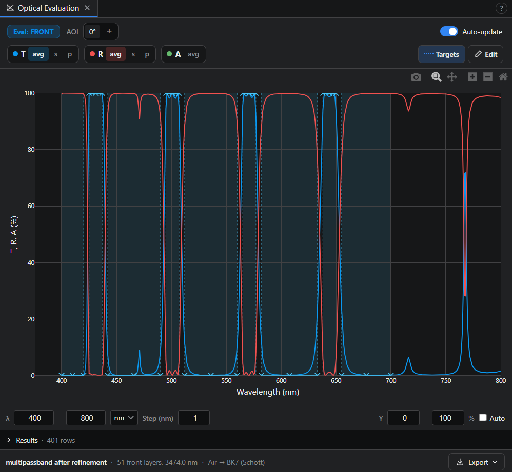
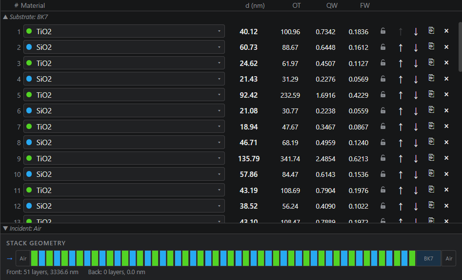
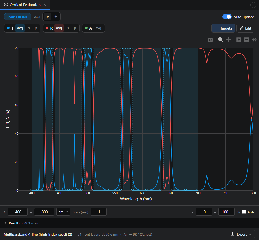
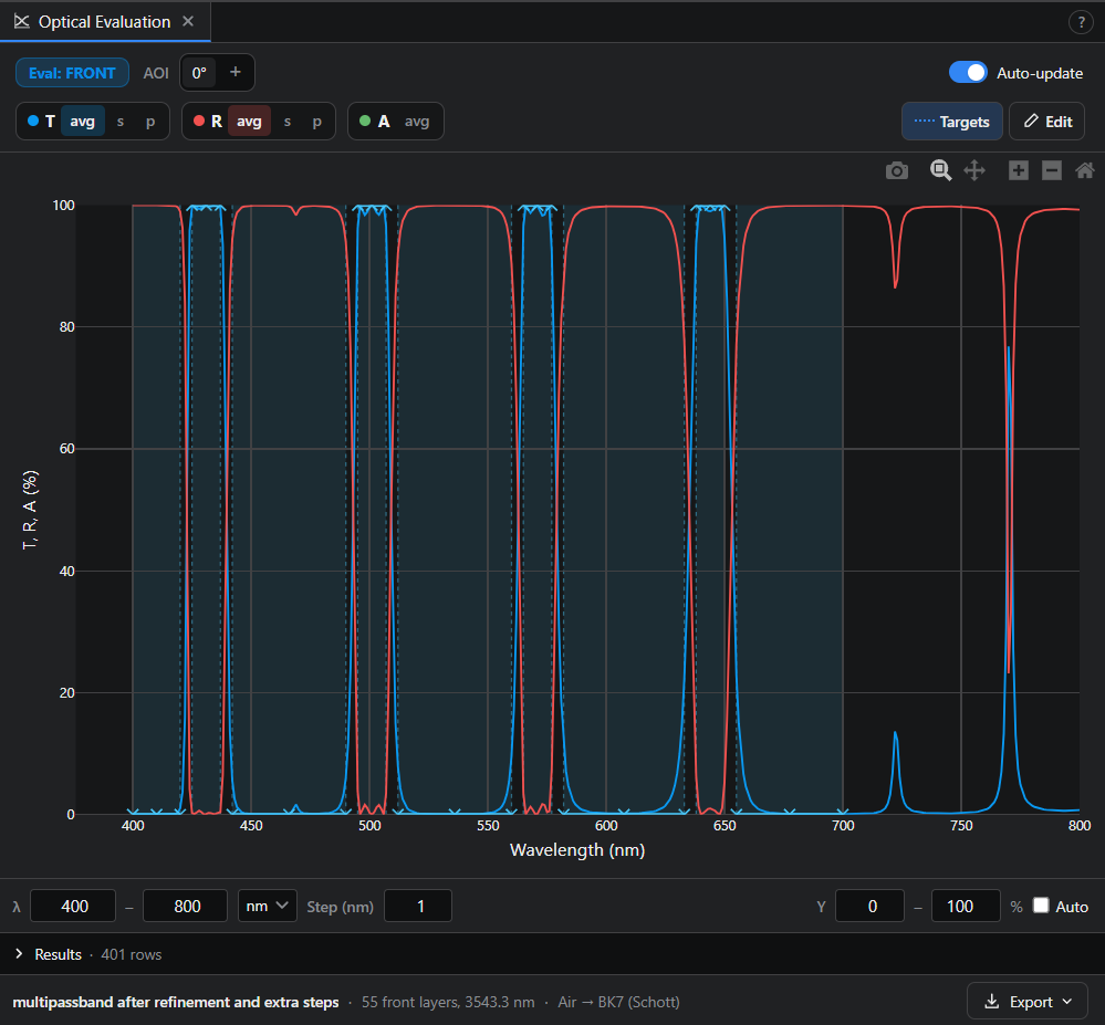
I noticed that it has a transmittance leak near 473 nm, in the 442–490 nm stopband, that I'd like to eliminate before stopping. Then I went on and optimized it further using the same 3 steps: Needle Automatic with Max layers set to 69, then Design Cleaner, then refinement using SQP again. That way I got to an even better result:
The result
That second round costs ten layers and more than halves the merit function. The whole thing, from opening the seed to saving this design, took about eight minutes.
The final design has 55 layers, strictly alternating TiO₂ and SiO₂, with TiO₂ against both the substrate and the air. Total physical thickness is 3460.90 nm, more than the seed: every refinement after the needle grew the layers, and nothing in the merit function asks for less material. The thinnest layer is 30.00 nm and the thickest 176.14 nm. The merit function is 0.014423, forty times better than the bare seed.
| Seed | After needle | After cleaner | After SQP | Final | |
|---|---|---|---|---|---|
| Layers | 1 | 101 | 45 | 45 | 55 |
| Total thickness | 2500.00 nm | 2801.73 nm | 3093.34 nm | 3253.63 nm | 3460.90 nm |
| Thinnest layer | n/a | 1.00 nm | 5.00 nm | 30.00 nm | 30.00 nm |
| MF | 0.581064 | 0.024512 | 0.017188 | 0.030352 | 0.014423 |
The Needle window reads 0.024327 for the needle design. This table uses the Merit Function Editor's figures.
Band by band, using the operand values the merit function itself is built from:
| Band | Target | Achieved average | Worst point in band |
|---|---|---|---|
| 425–437 nm | 1 | 99.514% | 99.018% at 437 nm |
| 495–507 nm | 1 | 99.429% | 97.594% at 507 nm |
| 565–577 nm | 1 | 98.702% | 93.207% at 577 nm |
| 638–650 nm | 1 | 97.579% | 89.641% at 638 nm |
| 400–420 nm | 0 | 0.012% | 0.239% at 420 nm |
| 442–490 nm | 0 | 0.488% | 13.998% at 490 nm |
| 512–560 nm | 0 | 0.892% | 11.190% at 560 nm |
| 582–633 nm | 0 | 2.400% | 24.264% at 633 nm |
| 655–700 nm | 0 | 1.954% | 26.105% at 655 nm |
Every stopband maximum sits on the band edge that faces a passband, and every passband minimum sits on the edge facing a stopband. Those points are the filter edges rolling off inside the 5 nm guard region, with the tail of the roll-off reaching a little way into the specified band. Trim 5 nm off each stopband end and the worst leakage anywhere in the design drops from 26.1% to 5.21%. If those edges need to be sharper, the guard bands are what to tighten, and the design will spend layers doing it.
Measured as lines rather than as bands, on a 0.1 nm grid:
| Target band | Peak | FWHM | Half-max range |
|---|---|---|---|
| 425–437 nm | 99.87% | 15.2 nm | 423.6–438.8 nm |
| 495–507 nm | 99.95% | 17.5 nm | 491.8–509.3 nm |
| 565–577 nm | 100.00% | 16.6 nm | 562.6–579.3 nm |
| 638–650 nm | 100.00% | 17.8 nm | 635.2–653.0 nm |
Each line is flat-topped with a little ripple rather than a single peak, which is what a band-average TAV target asks for. Nothing in the merit function rewards a smooth top, only a high average, so if flatness matters the target should say so.
The plot also runs up to 31.72% at 762 nm, well outside the specified range. Nothing was ever asked of the design above 700 nm, so nothing constrains it there. If out-of-band blocking matters for the application, it has to be specified. The merit function is the whole of what the optimizer knows.
What each stage contributed
Needle created the structure. It chose how many layers the filter needs and in what order, starting from a design that had none of that information in it. Neither Design Cleaner nor SQP could have produced this topology, and neither could refinement of any hand-built stack.
Design Cleaner removed what the search left behind. Synthesis is exploratory, and exploration leaves clutter, so the cleanup step is what turns a search result into a design.
SQP made the design buildable. The 30 nm floor is a manufacturing statement, and applying it as a constraint after the structure was settled, rather than as a limit during synthesis, is what let the design keep its structure while respecting it. The floor still cost merit, and the second round won it back.
The order matters as much as the tools. Constrain too early and synthesis never finds the structure. Clean too early and you delete layers the search still needs.
What this result does not yet show
The design was optimized at normal incidence, average polarization, one coated surface, and the stated TiO₂/SiO₂ dispersion. It has not been checked at oblique incidence, where narrow lines shift toward the blue and split between s and p. It has not been checked against deposition errors either, and a 55-layer filter with 30 nm layers is the kind of design where thickness tolerance decides whether it can be made at all. A second Needle run from the same seed can also land on a different local minimum with a different layer count.
Those are the subjects of the tolerancing and monitoring tutorials. A synthesized design is the start of that work, not the end of it.